With growing concern about low cost clean energy, solar power has again become a focal point for alternatives to fossil fuel energy production.
Solar panels employ photovoltaic cells to generate current flow. When a photon hits silicon, the photon is transmitted through the silicon, reflected off the surface, or absorbed by the silicon if the photon energy is higher than the silicon band gap value. This generates an electron-hole pair and sometimes heat, depending on the band structure. The greater the absorption the greater the efficiency of the cell.
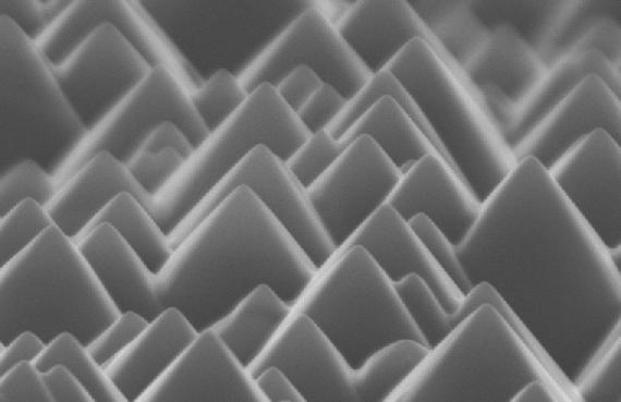
Generally, the solar panels are flat; however, textured structures have more adsorption efficiency.
It is challenging to produce textured structures for solar panels. One such problem includes the formation of a bottom electrode. A bottom electrode deposition occurs by forming a thick layer of electrode material and deep reactive ion etching (DRIE) the material to attempt to conform the bottom electrode material to the shape of the underlying structure. DRIE is a highly anisotropic etch process making the formation of the bottom electrode highly sensitive to thickness variations. A bottom electrode that is too thin results in series resistance problems and affects the efficiency of the solar cell.
IBM has developed an improved method for fabricating a photovoltaic device structure with a textured electrode.

The method includes forming a plurality of pillar structures in a substrate, forming a first electrode layer on the pillar structures and forming a continuous three-dimensional (3D) photovoltaic stack including an N-type layer, a P-type layer and an intrinsic layer on the first electrode. Then, a second electrode layer is deposited over the photovoltaic stack such that gaps or fissures occur in the second electrode layer between the pillar structures. The second electrode layer is wet etched to open up the gaps or fissures and reduce the second electrode layer to form a three-dimensional electrode of substantially uniform thickness over the 3D photovoltaic stack.
Publication number: US 20160204286
Patent Title: THREE-DIMENSIONAL CONDUCTIVE ELECTRODE FOR SOLAR CELL
Publication date: Jul 14, 2016
Filing date: Mar 22, 2016
Inventors: KEITH E. FOGEL; AUGUSTIN J. HONG; JEEHWAN KIM; DEVENDRA K. SADANA;
Original Assignee: NTERNATIONAL BUSINESS MACHINES CORPORATION
