In what may be a breakthrough in LED displays, NASA has invented a way to grow red, green, and blue colored LEDs all on a single semiconductor wafer. This
Currently, to fabricate LEDs of different colors, semiconductors having different crystal structures are needed. Red LEDs require a cubic zinc blende crystal structure while higher energy colors like Green/Blue require a hexagonal wurtzite crystal structure.
However, because of the difference in atomic crystal structures integration and fabrication of Red and Green/Blue LEDs on one wafer has been extremely difficult. As a result, manufacturing of high definition (HD) LED display panels has been expensive and also creates a barrier to higher resolution displays.

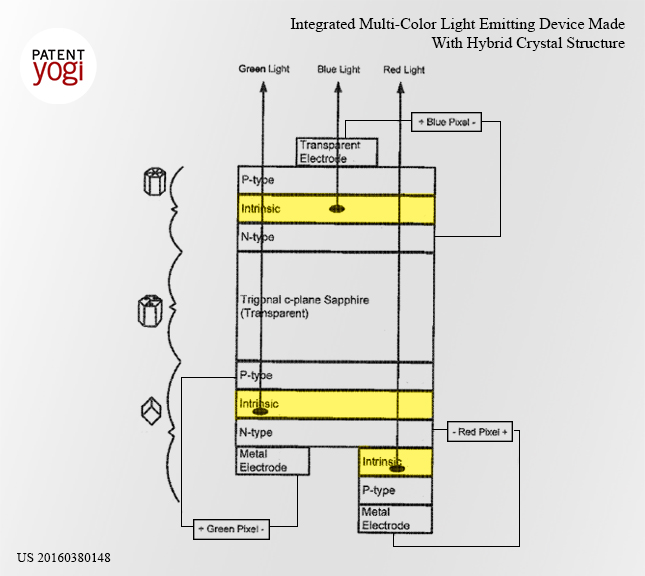
NASA has now invented a way to fabricate multi-color light emitting device on a single wafer of sapphire by growing Red LED on one side of the sapphire and Green and Blue on the opposite side.
Accordingly, a double-sided hetero crystal with hexagonal wurtzite III-Nitride compound semiconductor is grown on one side and cubic zinc-blended III-V or II-VI compound semiconductor on the opposite side.
The bandgap energy and lattice constant may be engineered by changing the alloy composition within the cubic group IV, group III-V, and group II-VI semiconductors and within the hexagonal III-Nitrides. Accordingly, different colors of light may be produced.
The impact of this technology is that color pixels comprising individual Red, Green and Blue LEDs can now be packed in densities that are far higher than in existing displays. This may pave the way to go beyond Ultra HD LED displays.
Publication number: US 20160380148
Patent Title: Integrated Multi-Color Light Emitting Device Made With Hybrid Crystal Structure
Publication date: 29 Dec 2016
Filing date: 13 Sep 2016
Inventors: Yeonjoon Park; Sang Hyouk Choi;
Original Assignee: U.S.A. as represented by the Administrator of the National Aeronautics and Space Administration

