Boeing has solved an enormous problem in manufacturing nanotube based electronics. This can now pave the way for extremely powerful processors unheard of so far.
Carbon nanotubes are excellent for use as conducting paths in electronic circuits. But fabrication of devices using carbon nanotubes is prohibitive in terms of time and cost because the nanotubes need to be individually positioned to form electrical connections.
This is similar to building a structure with a set of lego blocks which need to be put in place one by one.
Now imagine if you could just dump all lego blocks together and they all self-assembled together to form the desired structure.
That’s exactly what Boeing has achieved with this patent.
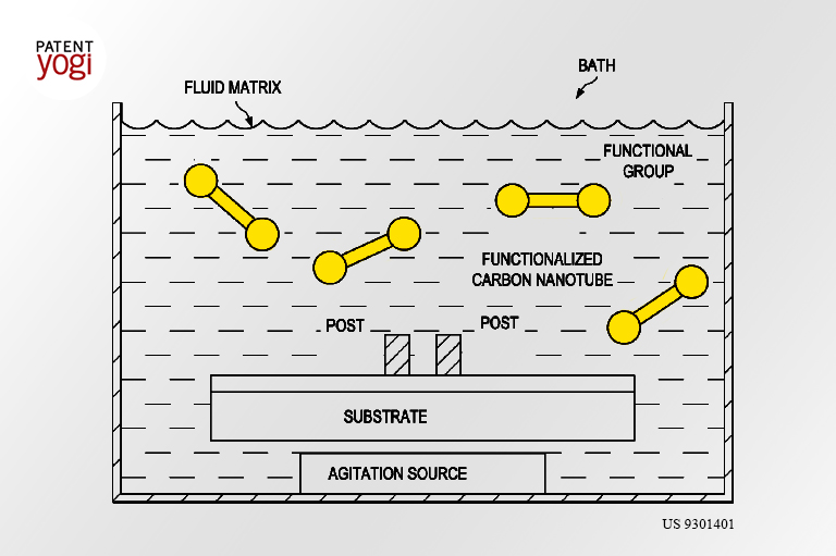
The invention uses the attraction force of chemical bonds to cause nanotubes to automatically place themselves in between contact terminals of a circuit.
Through a chemical process, the ends of the nanotubes are attached with a functional group to yield functional nanotubes.
A fluid matrix of the functional nanotubes is then poured over a substrate containing the semiconductor device. The substrate may have contact terminals which are not yet connected to form the complete circuit.
Once the functional nanotubes come in contact with the substrate, the ends of the nanotubes are attracted to the contact terminals and adhere. This forms the required electrical connection without any separate aligning force.
Publication number: US 9301401
Patent Title: Nanotube electronics templated self-assembly
Publication date: 29 Mar 2016
Filing date: 6 Aug 2015
Inventors: Keith Daniel Humfeld
Applicant: The Boeing Company
